HDI PCB Manufacturing Process
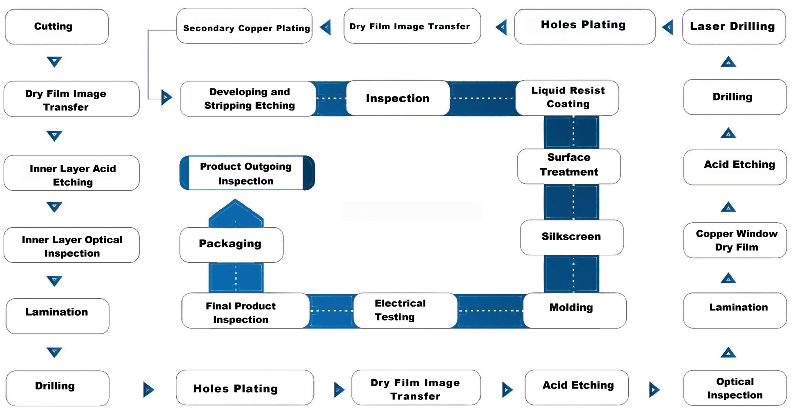
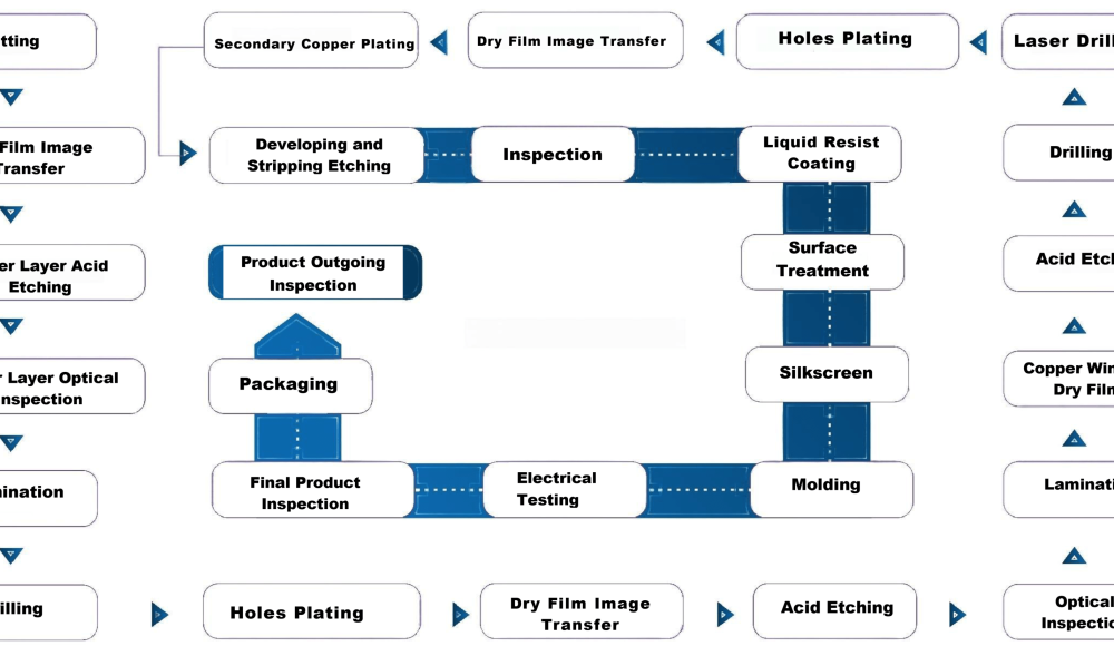
- Cutting: Raw material (typically copper-clad laminate) is cut into panels of required sizes for processing.
- Dry Film Image Transfer: A photosensitive dry film is applied to the copper surface. The film is then exposed to UV light through a photo-mask, which transfers the circuit design onto the film.
- Inner Layer Acid Etching: Precise etching and cleaning processes to remove excess copper, forming clear circuit paths of the PCB.
- Inner Layer Optical Inspection: The etched inner layers are inspected using automated optical inspection (AOI) systems to detect any defects in the circuitry.
- Lamination: Multiple inner layers are bonded together with prepreg (pre-impregnated with resin) layers and outer copper layers to form a multi-layer PCBs. Precise lamination and bonding techniques is utilized to ensure the adhesion strength and stability of multi-layer boards.
- Drilling: Holes for vias and through-hole components are drilled into the laminated PCB stack using precision drilling equipment, enhancing hole conductivity and reliability through plating processes.
- Hole Plating: The drilled holes are chemically plated with a thin layer of copper to create conductive pathways between the different layers of the PCB.
- Secondary Copper Plating: Additional copper is electroplated onto the surface and through-holes to ensure adequate conductivity and durability.
- Dry Film Image Transfer (Outer Layer): Similar to the inner layers, a photosensitive dry film is applied to the outer layers, exposed to UV light through a photo-mask, and developed to create the outer precise circuit patterns ensuring circuit pattern accuracy.
- Developing and Stripping Etching: The developed film is removed, and the exposed copper is etched away, leaving behind the final circuit pattern on the outer layers.
- Inspection: Another round of inspection (often AOI) to ensure the outer layer patterns are correct and free of defects.
- Liquid Resist Coating: A liquid photo-resist is applied to the PCB to protect certain areas during the surface finish process.
- Surface Treatment: Surface finishes such as HASL (Hot Air Solder Leveling), ENIG (Electroless Nickel/Immersion Gold), OSP, soft gold plating, hard gold plating, and lead-free HASL or others are applied to protect the exposed copper and to improve the durability and performance of circuit boards.
- Characters (Silkscreen): Identifying marks, labels, and component outlines are printed onto the board using silkscreen printing.
- Shaping: The PCB is routed or punched to achieve its final shape and size, including cutting out any internal slots or contours.
- Electrical Testing: The PCB undergoes electrical testing (e.g., flying probe or in-circuit testing) to verify continuity and isolation, ensuring all connections are correct.
- Final Product Inspection: A thorough final inspection to check for any physical or electrical defects before shipping, ensuring each circuit board meets customer specifications and standards.
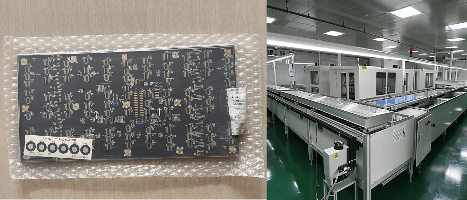
- Packaging: The PCBs are carefully packaged to prevent damage during transit.
- Product Outgoing Inspection: The packaged products are inspected one last time to ensure they meet quality standards and customer specifications before being shipped out.
