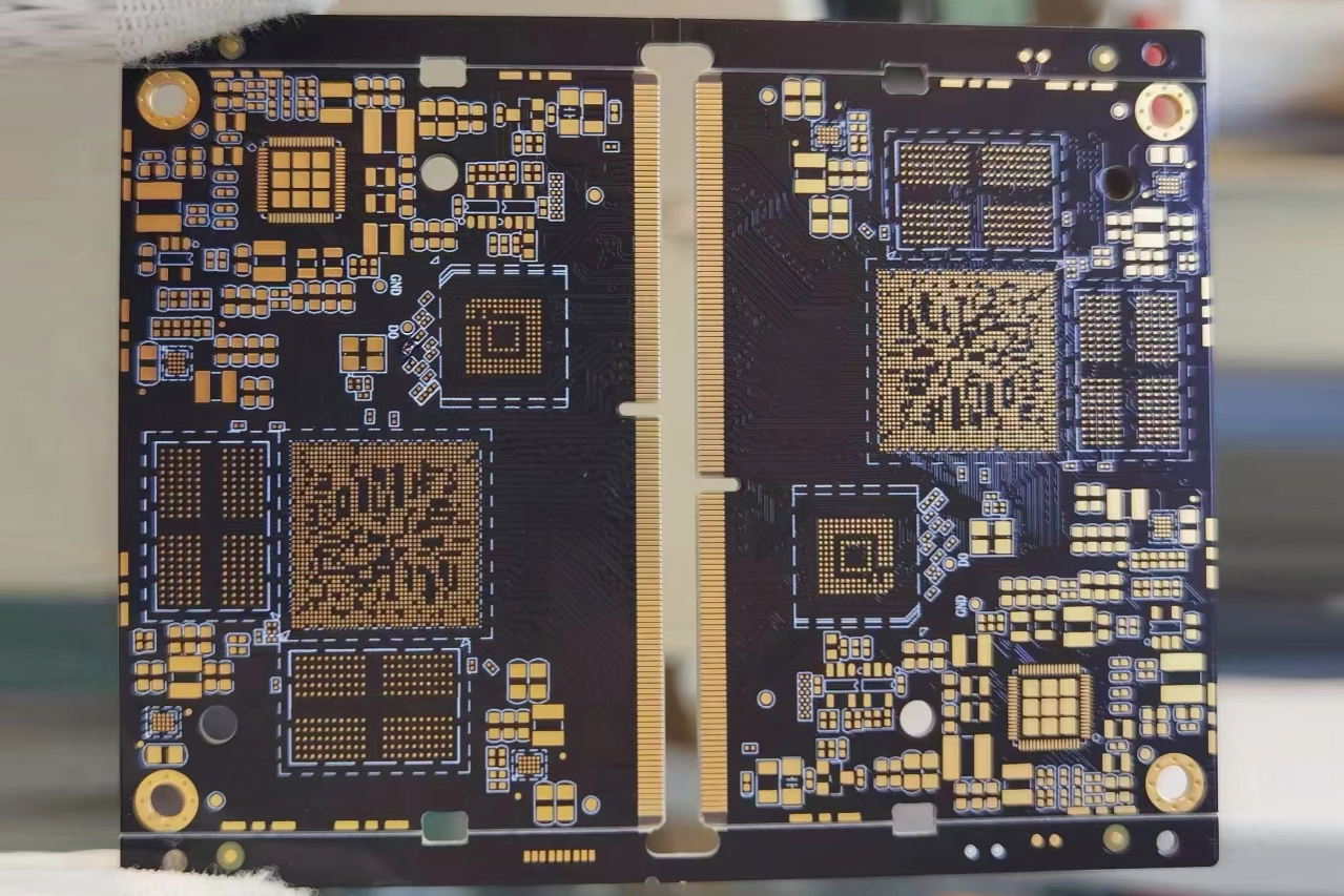
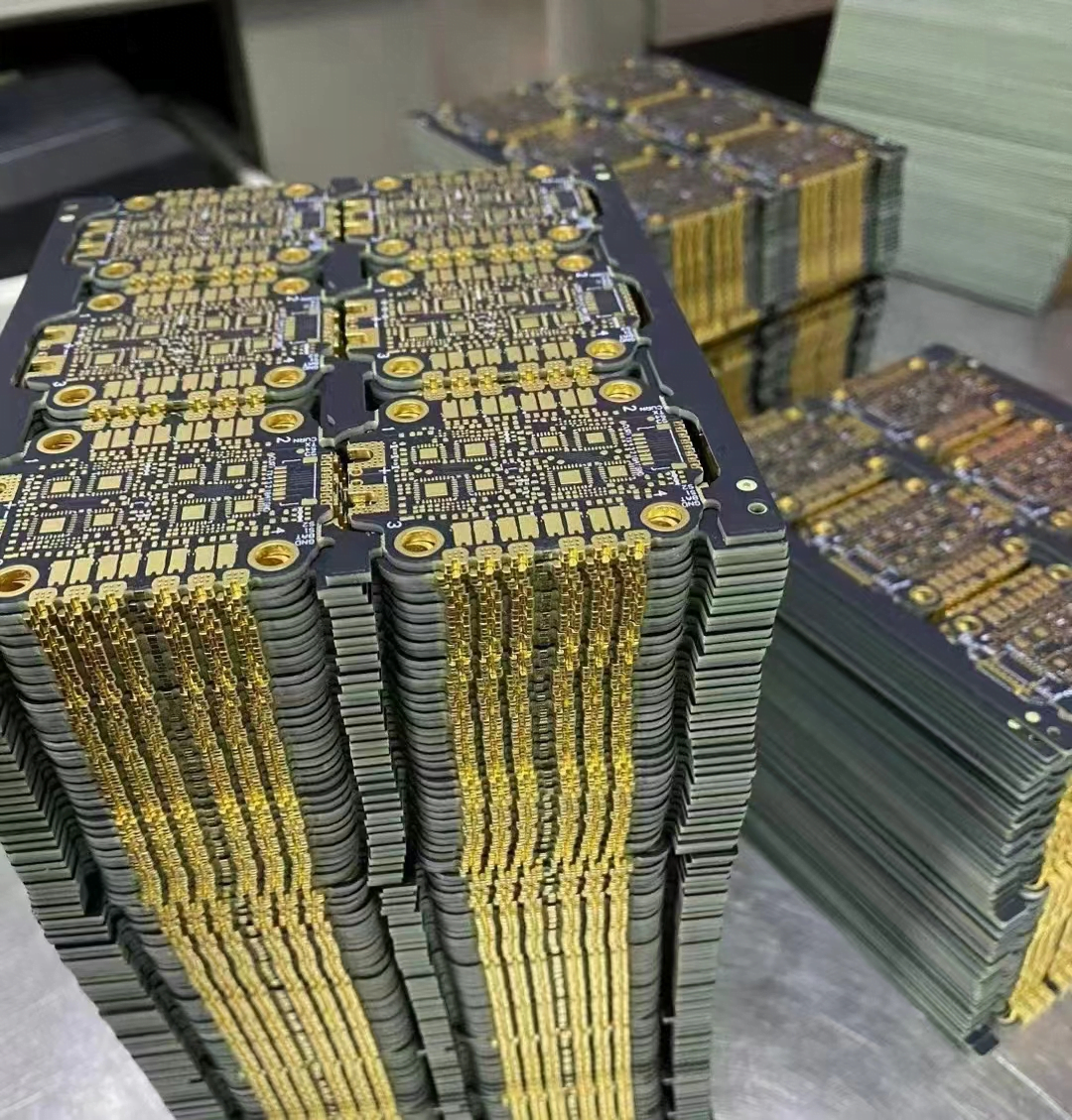
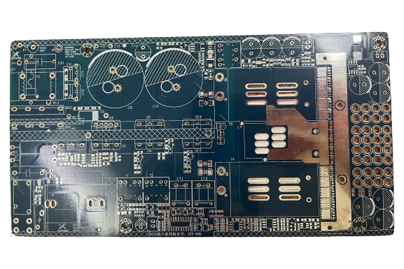
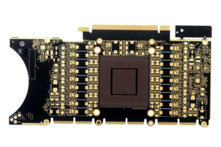
HDI PCBs Introduction
HDI PCBs are characterized by its high circuit density, allowing for more functionality and complex designs to be integrated into a limited space. HDI PCBs are a key technology in modern electronic product design and manufacturing, representing the forefront of printed circuit board design and manufacturing capabilities.
Advantages of HDI PCBs
- High Density Design: HDI PCBs utilize finer lines and spacing, smaller vias, and capture pads, enabling more components and signal paths to be integrated into a smaller area.
- Multi-layer Structure: They typically contain more layers, facilitating complex multi-layer interconnections and distribution, suitable for high performance applications.
- Blind and Buried Vias: HDI PCBs use blind and buried via technology, which increases layer-to-layer interconnections and further enhances board density and performance.
- Higher Signal Transmission Speed: Due to shorter signal paths and higher signal integrity, HDI PCBs support higher signal transmission speeds and frequencies.
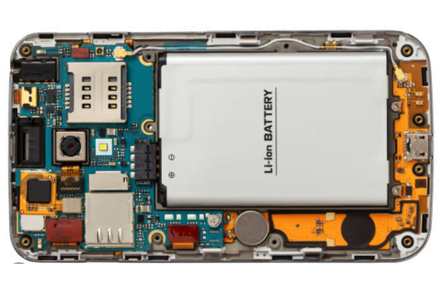
- Smaller Size and Weight: They are ideal for applications requiring lightweight and miniaturized designs, such as smartphones, tablets, and wearable devices.
- High Reliability: HDI PCBs generally offer high reliability and low failure rates due to their precise manufacturing processes and designs.
Application Areas
High density interconnect pcb are widely used in various fields that require high performance and high density circuit designs, including:
Consumer electronics (e.g., smartphones, tablets, laptops)
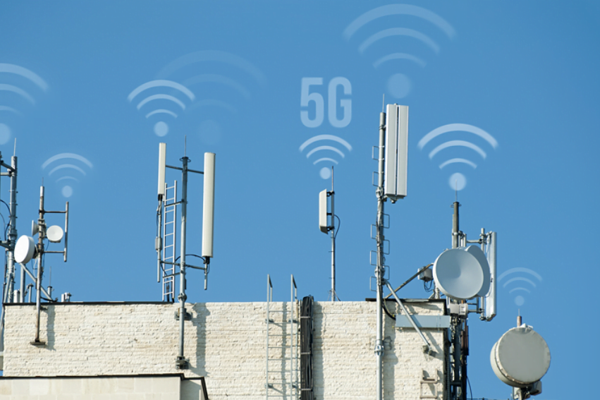
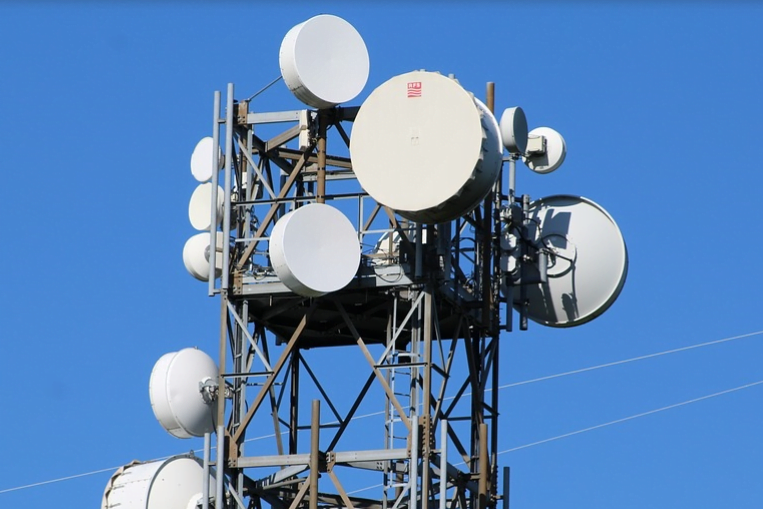
Communication devices (e.g., 5G base stations, routers, switches)
Industrial control systems (e.g., automation equipment, robotics)
Medical equipment (e.g., MRI machines, CT scanners)
Automotive electronics (e.g., autonomous driving systems, in-car entertainment systems)
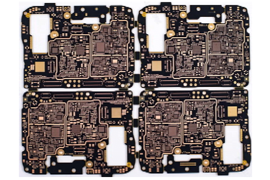
| Smartphone Boards | |
|---|---|
| Purpose | Smartphone |
| Applicable Field | Communication Equipment |
| Layers | 10 Layers (10L) (2+6+2) |
| Board Thickness | 0.8 mm (±0.05 mm tolerance) |
| Minimum Line Width/Spacing | 45/50 μm (±5 μm tolerance) |
| Surface Treatment | Chemical Gold + OSP (Organic Solderability Preservative) |
| Special Features | Buried Via Design |
| Operating Temperature Range | -40°C to +85°C |
| Electrical Conductivity | ≥58 MS/m (millisiemens per meter) |
| Thermal Conductivity | 0.22 W/mK (watts per meter-kelvin) |
| Dielectric Constant | 4.5 (at 1 GHz) |
| Dissipation Factor | 0.015 (at 1 GHz) |
| Signal Integrity | High signal integrity with controlled impedance design |
| Mechanical Properties | High durability and flexural strength suitable for high-stress environments |
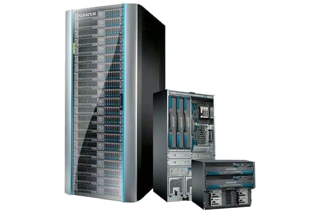
| High-Speed Board | |
|---|---|
| Purpose | Server Motherboard |
| Applicable Field | Data/Server |
| Layers | 14 Layers (14L) |
| Board Thickness | 2.4 mm (±0.1 mm tolerance) |
| Outer Layer Copper Thickness | 45-65 μm (±5 μm tolerance) |
| Special Design | POFV (Pin-in-Paste Over Fill Via), Back Drilling, High-Speed Board Material Lamination |
| Minimum Line Width/Spacing | 0.1 mm ±20% / 0.1 mm ±20% |
| Surface Treatment | Immersion Tin |
| Operating Temperature Range | -55°C to +125°C |
| Electrical Conductivity | ≥58 MS/m (millisiemens per meter) |
| Thermal Conductivity | 0.25 W/mK (watts per meter-kelvin) |
| Dielectric Constant | 3.8 (at 1 GHz) |
| Dissipation Factor | 0.008 (at 1 GHz) |
| Signal Integrity | Excellent signal integrity with controlled impedance and low loss characteristics |
| Mechanical Properties | High rigidity and flexural strength, suitable for heavy-duty server applications |
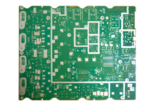
| High-Frequency Microwave Board | |
|---|---|
| Purpose | 5G Antenna |
| Applicable Field | Communication Equipment |
| Layers | 10 Layers (10L) |
| Board Thickness | 2.8 mm (±0.1 mm tolerance) |
| Minimum Line Width | 102 μm (±10 μm tolerance) |
| Surface Treatment | Electroless Nickel Immersion Gold (ENIG) |
| Operating Temperature Range | -40°C to +85°C |
| Electrical Conductivity | ≥58 MS/m (millisiemens per meter) |
| Thermal Conductivity | 0.25 W/mK (watts per meter-kelvin) |
| Dielectric Constant | 3.7 (at 1 GHz) |
| Dissipation Factor | 0.005 (at 1 GHz) |
| Signal Integrity | High signal integrity with low loss characteristics suitable for high-frequency applications |
| Mechanical Properties | High rigidity and flexural strength, suitable for high-stress environments |
| Impedance Control | Controlled impedance with ±5% tolerance |
| Copper Weight | 1 oz (outer layers), 1 oz (inner layers) |
| Special Features | High-frequency laminate, via in pad, low loss dielectric material |
| High-Frequency Buried Copper Board | |
|---|---|
| Purpose | Communication Base Station |
| Applicable Field | Communication Equipment |
| Layers | 6 Layers (6L) |
| Board Thickness | 3.0 mm (±0.1 mm tolerance) |
| Minimum Line Width | 0.25 mm (±0.02 mm tolerance) |
| Surface Treatment | Electroless Nickel Immersion Gold (ENIG) |
| Special Processes | Blind Slot + Through Slot (tolerance ±0.1 mm) + Double-Sided Back Drilling (tolerance ±0.05 mm) |
| Operating Temperature Range | -40°C to +105°C |
| Electrical Conductivity | ≥58 MS/m (millisiemens per meter) |
| Thermal Conductivity | 0.30 W/mK (watts per meter-kelvin) |
| Dielectric Constant | 3.5 (at 1 GHz) |
| Dissipation Factor | 0.004 (at 1 GHz) |
| Signal Integrity | High signal integrity with controlled impedance and low loss characteristics |
| Mechanical Properties | High rigidity and flexural strength, suitable for high-stress environments |
| Impedance Control | Controlled impedance with ±5% tolerance |
| Copper Weight | 1 oz (outer layers), 1 oz (inner layers) |
| Frequency Range | Suitable for high-frequency applications up to 40 GHz |
| Via Plating | High-quality copper plating in vias for improved reliability and conductivity |
| Environmental Compliance | RoHS and REACH compliant |
| Product Details | Medical Instrument Boards |
|---|---|
| PCB Name | 6L 2+N+2 HDI PCB |
| Material | FR-4, TG170 |
| Board Layer | 6 Layers (6L) |
| Board Thickness | 2.0 mm (±0.1 mm tolerance) |
| Finished Outer Copper Weight | 2 oz Finished |
| Internal Copper Weight Inner | 2 oz Base |
| Solder Mask | Black Solder Mask |
| Smallest Hole Size | 0.1 mm (±0.02 mm tolerance) |
| Blind/Burried Vias | Yes, Requested |
| Application | Medical Devices Product |
| Operating Temperature Range | -55°C to +125°C |
| Electrical Conductivity | ≥58 MS/m (millisiemens per meter) |
| Thermal Conductivity | 0.22 W/mK (watts per meter-kelvin) |
| Dielectric Constant | 4.2 (at 1 GHz) |
| Dissipation Factor | 0.015 (at 1 GHz) |
| Signal Integrity | High signal integrity with controlled impedance |
| Mechanical Properties | High durability and flexural strength suitable for high-stress environments |
| Automotive Electronics Boards | |
|---|---|
| Applicable Field | New Energy Vehicles |
| Layers | 4 Layers (4L) |
| Base Material | S1000-2M, High Temperature Resin |
| Board Thickness | 6.0 mm (±0.1 mm tolerance) |
| Minimum Hole Diameter | 3.0 mm (±0.05 mm tolerance) |
| Minimum Line Width | 0.25 mm (±0.02 mm tolerance) |
| Inner Layer Copper Thickness | 5.0 mm (±0.05 mm tolerance) |
| Surface Treatment | Chemical Gold (Au: 0.05-0.075 μm) |
| Special Processes | Control Depth Drilling (±0.1 mm precision), Slotting, Compression |
| Operating Temperature Range | -40°C to +125°C |
| Electrical Conductivity | ≥58 MS/m (millisiemens per meter) |
| Thermal Conductivity | 0.25 W/mK (watts per meter-kelvin) |
| Dielectric Constant | 4.2 (at 1 GHz) |
| Dissipation Factor | 0.02 (at 1 GHz) |
| Mechanical Properties | High durability and flexural strength suitable for high-stress environments |
| Impedance Control | Controlled impedance with ±5% tolerance |
| Environmental Compliance | RoHS and REACH compliant |

