HDI PCB in LED Screens
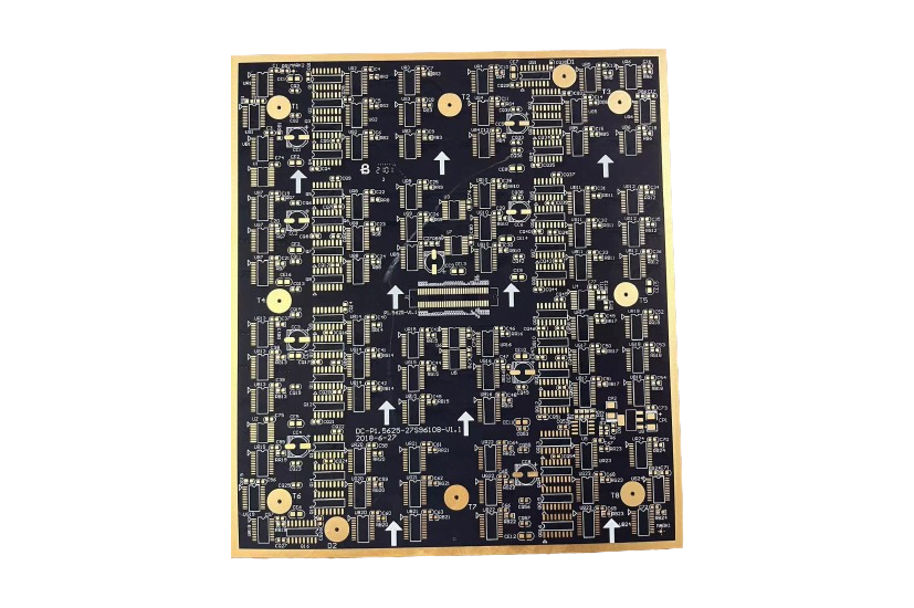
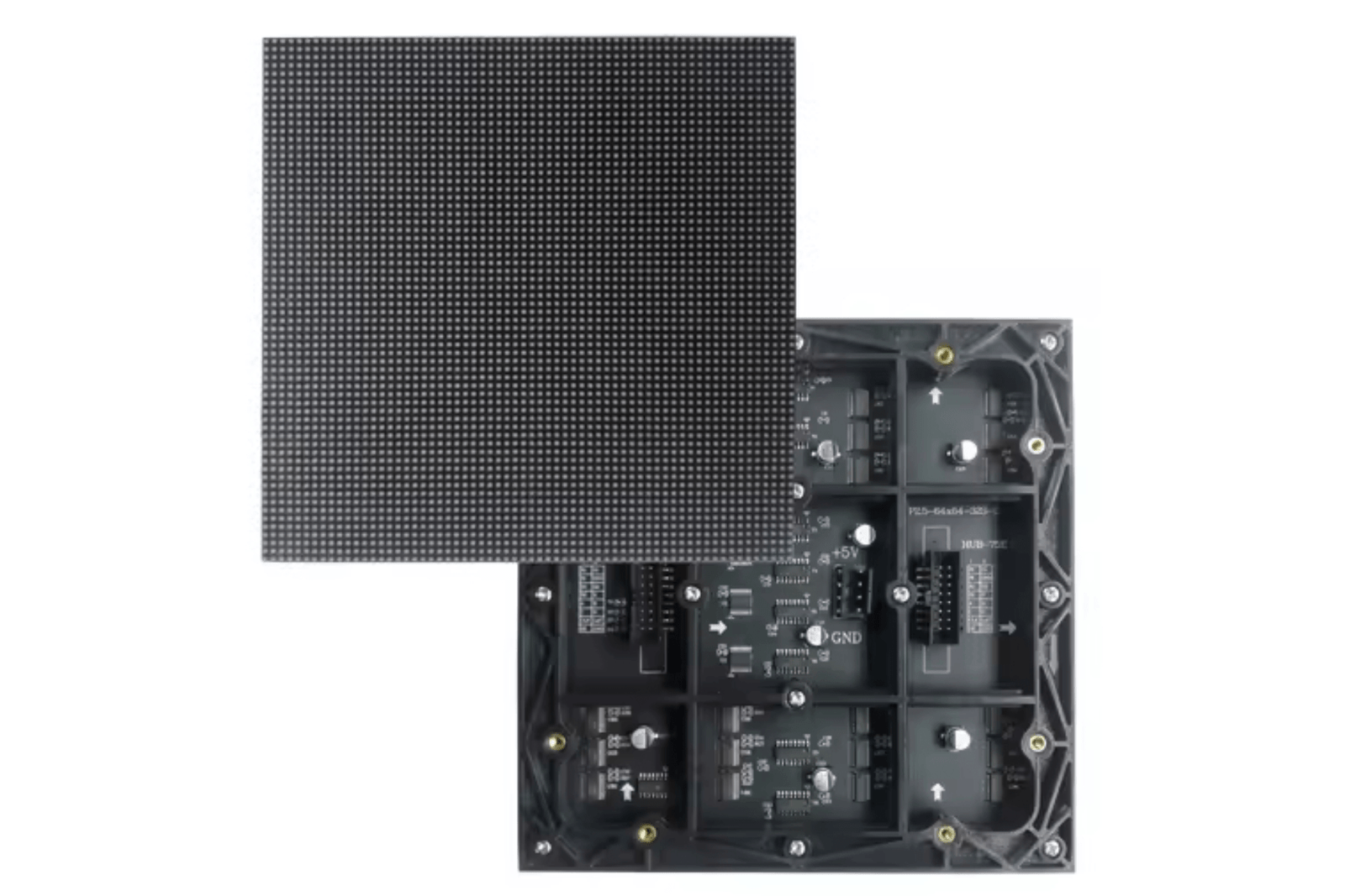
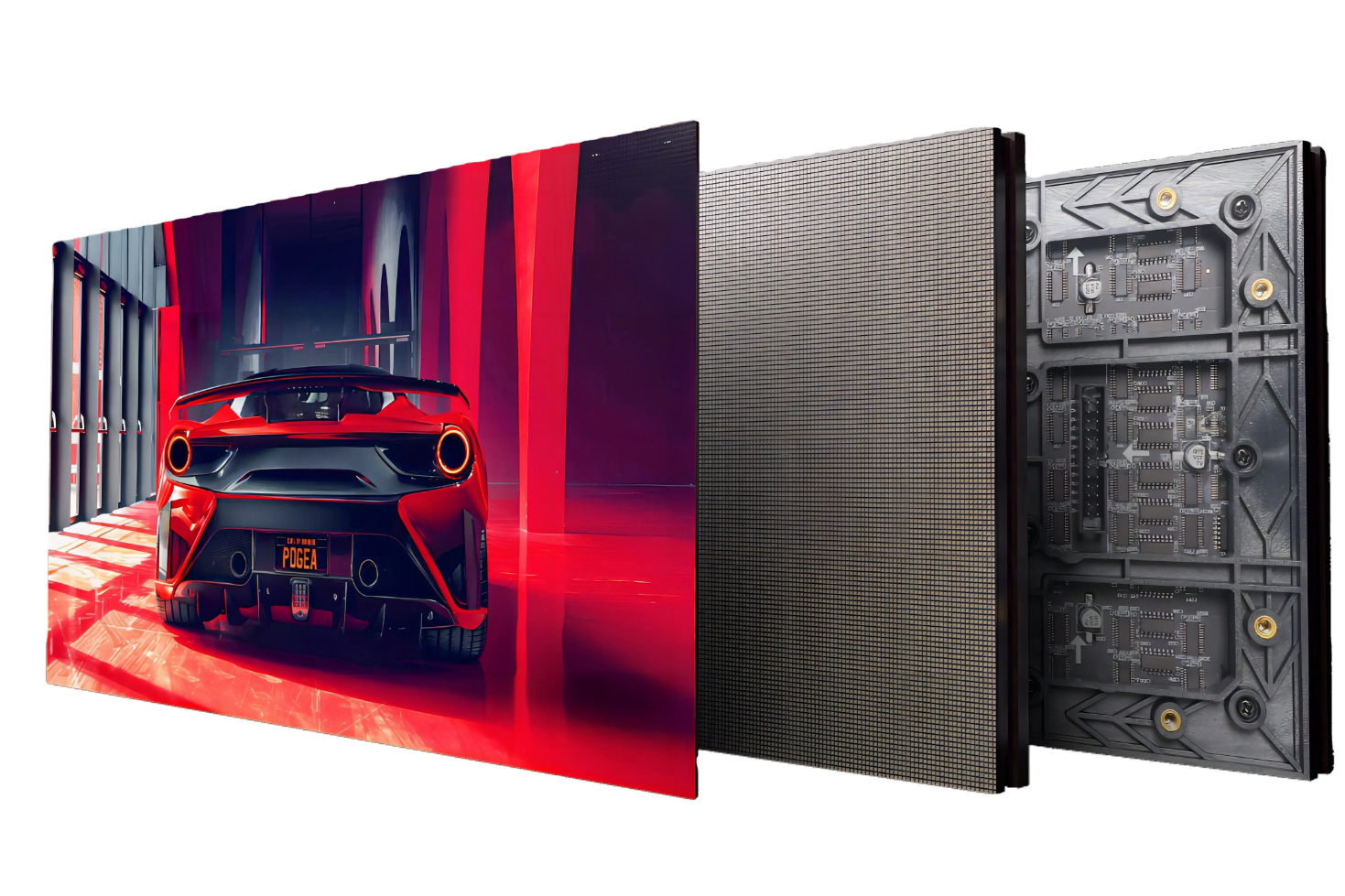
HDI PCBs play a crucial role in the design and manufacturing of modern LED screens, including those used in televisions, digital displays, and large video walls, providing compactness, performance, and reliability, meeting the demands of modern display applications. Here are the reasons and advantages of HDI PCBs in LED screens:
Compact Design: HDI PCBs allow more electronic components to be integrated into smaller areas. This compactness is particularly important for LED screens with limited space, enabling thinner and lighter designs, which are highly favored in consumer electronics.
Performance Enhancement: HDI PCBs support higher signal transmission speeds and frequencies, which is crucial for LED screens that need to process high definition signals quickly and efficiently. This ensures smooth video playback and overall performance improvement.
Higher Component Density: LED screens require a large number of small components, such as LEDs, drivers, and controllers, which need to be tightly packed. HDI technology allows for higher component density, improving screen resolution and brightness while maintaining a slim design.
Better Heat Dissipation: With the increase in component density, heat management becomes a challenge. HDI PCBs can include advanced thermal management features, effectively dissipating heat to ensure the longevity and reliability of LED screens.
Enhanced Reliability: The manufacturing precision and advanced processes of HDI PCBs bring high reliability and low failure rates. This is particularly important for LED screens that need to operate for long periods without failure. The precise manufacturing processes and highquality materials of HDI PCBs provide greater reliability and durability, making them suitable for various harsh working environments, ensuring the longterm stable operation of LED screens.
Advanced Interconnect Technology: HDI PCBs use blind and buried vias, reducing the need for throughhole connections, allowing for more complex circuit routing. This is highly beneficial for managing the numerous pixels and driving circuits in LED screens.
Future Trends
As technology advances, the role of HDI PCBs in LED displays will continue to grow.We will see these trends of LED displays happen:
Further Miniaturization: Continuous improvements in PCB manufacturing will allow for smaller, more efficient components, further reducing the thickness and weight of LED displays.
Higher Resolution: With increasing consumer demand for higher resolutions (such as 4K and 8K), HDI PCBs will support the necessary highspeed signal processing and dense component arrangement.
Enhanced Durability: New materials and advanced manufacturing techniques will increase the durability and lifespan of LED displays, especially in outdoor and industrial applications.
| LED Boards | |
|---|---|
| Applicable Field | High Definition Display |
| Layers | 6 Layers (6L) 2-Stage HDI |
| Board Thickness | 1.28 mm (±0.05 mm tolerance) |
| LED Pitch | 1.25 mm (±0.02 mm tolerance) |
| LED Pad Size | 116.8 μm x 116.8 μm (±5 μm tolerance) |
| LED Pad Spacing | 53 μm (±3 μm tolerance) |
| Surface Treatment | Electroless Nickel Immersion Gold (ENIG) |
| Operating Temperature Range | -40°C to +85°C |
| Electrical Conductivity | ≥58 MS/m (millisiemens per meter) |
| Thermal Conductivity | 0.25 W/mK (watts per meter-kelvin) |
| Dielectric Constant | 4.2 (at 1 GHz) |
| Dissipation Factor | 0.02 (at 1 GHz) |
| Flammability Rating | UL94 V-0 |
| Signal Integrity | High signal integrity with controlled impedance |
| Mechanical Properties | High durability and flexural strength suitable for high-stress environments |
| Impedance Control | Controlled impedance with ±5% tolerance |
| Environmental Compliance | RoHS and REACH compliant |
| Lifespan | ≥50,000 hours |
| Power Consumption | ≤15 W (depending on the display size and brightness) |
| Viewing Angle | Horizontal/Vertical 160° |
| Brightness | 1000-5000 nits (adjustable based on application requirements) |
| Contrast Ratio | 3000:1 |
| Response Time | ≤2 ms |


