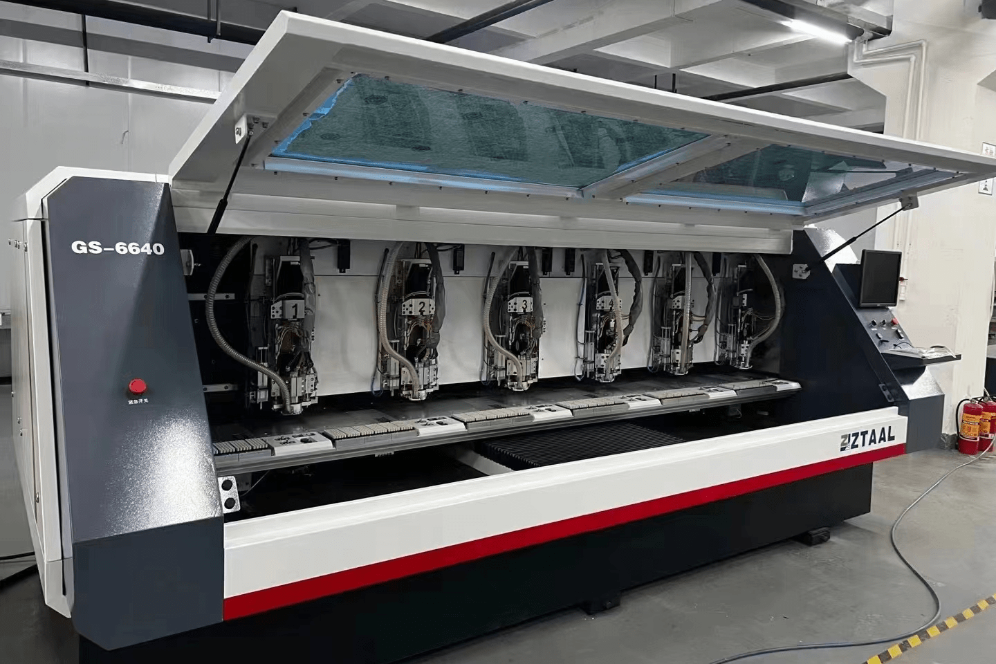
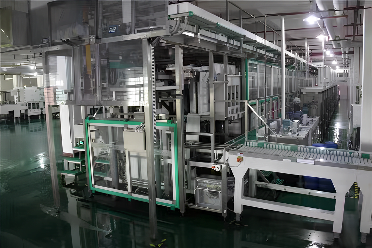
We produce PCB based on your GERBER file and provide useful suggestions to optimize PCBs design(Circuit Design/Layout Design), ensuring they meet design accuracy and manufacturing possibility.
| Type | Sample (days) | Mass Production (days) |
|---|---|---|
| Through Hole | 4-7 | 6-10 |
| HDI | 7-13 | 14-25 |
| Anylayer | 12-14 | 18-32 |
| High Frequency | ||
| High Speed | 5-8 | 6-12 |
| FPC | 5-10 | 8-16 |
| R&F | 10-18 | 20-28 |
| Metal Based | / | 6-12 |
Sample Producing/Prototyping
In terms of sample and small to medium batch production, the manufacturer showcases strong prototyping capabilities. The factory can quickly produce samples of varying complexity, including through-hole boards, HDI boards, high-frequency high-speed boards, etc. Advanced prototyping equipment can handle complex and high-density circuit board designs. Our prototype production cycle is short, typically completed within 7-13 days, depending on product type and complexity. We also provide small to medium batch production services to ensure products can be brought to market quickly.
Mass Production/Manufacturing
PCB manufacturing process covers all steps from material preparation to final product testing. The factories employ the most advanced production equipment and processes to ensure high-quality standards at every production stage.
The factory only select high-quality raw materials, including substrate materials and copper foil, to ensure product reliability and performance. For prototyping and mass-production the factory only use original boards such as Kingboard, Nanya (Taiwan), Shengyi, and ITEQ.
Process Capacity
| Item | MZ-HDI | JS-HDI | ||||
|---|---|---|---|---|---|---|
| Mass productoin | Small-lot/Sample | Mass productoin | Small-lot/Sample | |||
| Max.layer | 16 | 32 | 16 | 32 | ||
| Finished board thickness(mm) | 2.4 | 3.0 | Min 0.3 Max 2.4 | Min 0.25 Max 2.8 | ||
| Dielectric layer thickness(mm) | 0.035 | 0.025 | 28 | 25 | ||
| Laminate | FR4,BT,high-speed(low loss,ultra low loss) | FR4,BT,high-speed(low loss,ultra low loss) | ||||
| Base copper thickness | Innerlayer | Min:Hoz Max:2oz | Min:Hoz Max:2oz | Min HOZ Max 3oz | Min 0.33oz Max 4oz | |
| Outlayer | Min:0.33oz Max:2oz | Min:0.33oz Max:2oz | Min HOZ Max 3oz | Min 0.33oz Max 4oz | ||
| Min. borehole diameter | Blind via (mm) | 0.075 | 0.060 | 0.075 | 0.07 | |
| Buried via(mm) | 0.15 | 0.10 | 0.15 | 0.1 | ||
| Through hole(mm) | 0.15 | 0.10 | 0.15 | 0.1 | ||
| Hole diameter tolerance | PTH (mm) | ±0.05 | ±0.05 | ±0.05 | ±0.035 | |
| NPTH(mm) | ±0.03 | ±0.025 | ±0.05 | ±0.03 | ||
| Bore diameter of back drilled through hole(mm) | 0.25 | 0.2 | ||||
| Back drilling diameter(mm) | D+0.2 | D+0.15 | ||||
| Back drilling depth tolerance (mm) | ±0.05 | ±0.05 | ||||
| Back drilling stub(mm) | 0.05-0.25 | |||||
| Max.plating hole aspect ratio(laser) | 0.8:1 | 1:1 | ||||
| warping degree | ≤0.5% | ≤0.5% | ≤0.75% | ≤0.50% | ||
| CNC routing tolerance (mm) | ±0.1 | ±0.05 | ±0.1 | ±0.05 | ||
| S/M dam (mm) | 0.075 | 0.065 | 0.075 | 0.065 | ||
| Min.resin filled hole (mm) | 0.15 | 0.15 | 0.2 | 0.15 | ||
| Thickness diameter ratio of resin plug hole | 10:1 | 18:1 | 8:1 | 12:1 | ||
| Min.diameter of resistance welding plug hole(mm) | 0.2 | 0.15 | 0.2 | 0.15 | ||
| Thickness diameter ratio of resistance welding plug hole | 8:1 | 10:1 | 6:1 | 8:1 | ||
| Iimpedance tolerance | ±8% | ±7% | ±8% | ±6% | ||
| Min.line width/space (inner-layer)μm | 50/50 | 45/45 | 40/40 | 35/35 | ||
| Mini line width/space (out- layer)um | 50/50 | 45/50 | 40/40 | 35/35 | ||
| MinBGA pad (mm) | 0.17 | 0.15 | 0.17 | 0.15 | ||
| Min:BGA pitch (mm) | 0.325 | 0.3 | 0.325 | 0.3 | ||
| Max.board size (mm) | 400*280 | 400*280 | 500*280 | 500*280 | ||
| Surface treatment | OSP, ENIG, OSP+ENIG(selective), LFHAL, ENEPIG, gold plating | Gold melting. OSP, gold melting+OSP, electroplating soft gold, electroplating hard gold, nickel palladium, nickel palladium+OSP | ||||
| Special process | Sidewall metallization, half hole, countersunk hole, depth control drill, POFV | Depth control drill, countersunk hole, gold finger, POFV, side metal edging, half hole | ||||


